Introduction
Complementary metal oxide semiconductor (CMOS) is an Integrated circuit (IC). In the 1970s, an integrated circuit (IC) chip could only contain up to 10,000 transistors, and transistor feature lengths were over 1 m. For instance, the Motorola 6800 CPU has just 4100 transistors and a 6.0 m feature length. But the IC industries have seen a profound upheaval in less than 50 years. Today’s chips may have more than 10 billion transistors, while their feature lengths may only be 10 nm. More functions can now be placed in a chip because of the huge rise in transistor density. This means that a modern electrical device’s chip is smaller and more powerful at the same time. The basic element that powers electronic circuits is known as a CMOS device because the circuits on a standard chip are created by combining two types of complementary transistors.
A Brief History of CMOS
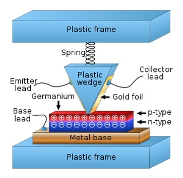
Vacuum tubes were used to create the first transistors, which were created in the early 1900s. Because of their size, vacuum tube transistors were challenging to utilise. In December 1947, John Bardeen, Walter Brattain, and William Shockley worked at the Bell Laboratory to create the point-contact germanium transistor. This transistor was significantly smaller, as seen in Figure 1. Additionally, it used far less electricity, ran at a lower temperature, and responded more quickly. This led to the solid-state transistor quickly displacing the vacuum tube transistor. Undoubtedly, the solid-state transistor is simpler to use. The electronic industries saw a significant upheaval very quickly after its debut. The three researchers from the Bell laboratory shared the 1956 Nobel Prize in Physics for their major contributions.

Point-contact transistor, CC0 1.0
Figure 1. A transistor with point contacts.
In 1954, Gordon Teal produced the first silicon transistors that were readily accessible for purchase. Since silicon performs better than germanium, silicon has steadily replaced germanium as the substrate material for transistors. The first transistor constructed of diffused silicon originally appeared in 1955. Epitaxy was put onto the transistor in 1960 in order to lower the collector’s resistance. Jean Hoerni put out the planar transistor in the same year.
Explore our latest online courses and learn new skills at your own pace. Enroll and become a certified expert to boost your career.
Metal Oxide Semiconductor Field Effect Transistor (MOSFET)
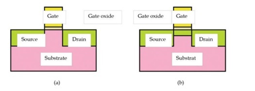
The MOSFET is used as an electronic switch or amplifier in circuits. The depletion-type MOSFET (D-MOSFET) and the enhancement-type MOSFET are the two types of MOSFETs (E-MOSFET). Figure 2 depicts the basic layout of both types of MOSFETs. The figure shows how similar the two gadgets are to one another. The drain, source, gate, and substrate terminals are among their four components. Physical separation exists between the source terminal and the E-drain MOSFET. The D-MOSFET, in contrast to the E-MOSFET, has a physical implant that connects the two terminals

Figure 2. Cross sections of an enhancement mode MOSFET and a depletion mode MOSFET, respectively.
The E- and D-MOSFETs function as an open switch and a closed switch, respectively, when no voltage is supplied to the gate terminal. This suggests that to turn the D-MOSFET off, power must be given to it. The E-MOSFET uses less power since it can be shut off without needing this extra voltage, which makes it popular in the IC sector. Consequently, the E-MOSFET is typically referred to as a MOSFET. A single crystal semiconductor layer, an oxide layer, and a polysilicon layer that acts as the gate terminal make up the device’s three main layers (i.e. the substrate). Aluminum was originally used to construct the gate terminal. The three layers of materials and the necessity of an electric field for the MOSFET to control its switching function are basically what gave rise to the moniker “MOSFET.” However, polysilicon was used as the gate material starting in the middle of the 1970s. The self-aligned source and drain terminals are created during ion implantation using the polysilicon gate’s exceptional temperature stability as a mask, which increases process precision. The name MOSFET is still used because it is so widely understood even though the gate is no longer made of aluminium.
CMOS Devices
Electronic circuits have independently used NMOS and PMOS transistors, but each has flaws of its own. When a logic 0 is needed, a PMOS transistor cannot provide an exact zero output voltage, but an NMOS transistor cannot produce a complete VDD value at the output when a logic 1 is needed. Circuitry power loss has occurred as a result of a partial swing from 0 to VDD. NMOS and PMOS transistors are combined in IC designs to address this issue. When, a logic 1 or 0 is to be formed, output VDS may be fully pushed up to VDD and pulled down to ground by connecting the sources of the PMOS transistor and the NMOS transistor to the VDD input voltage and the ground, respectively. The component of the circuit made up of PMOS transistors is therefore referred to as the pull-up network, whilst the segment made up of NMOS transistors is referred to as the pull-down network.

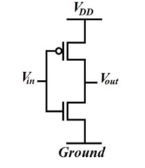
Figure 3. TCMOS inverter schematic diagram.
A complementary MOS circuit, often known as a CMOS circuit, is one that is made up of these two complementary transistors. In a CMOS circuit, only one of the pull-up or pull-down networks is ever used. Consider the workings of a CMOS inverter, such as the one in Figure 3. The NMOS transistor behaves as an open switch when a logic 1 is to be created at the output, but the PMOS transistor behaves as a closed switch. The PMOS and NMOS transistors respond similarly, acting as an open and a closed switch, respectively, when a logic 0 has to be created. This permits nearly negligible power loss while the circuit is operating in steady state.
Conclusion
In this tutorial, we have learned about Complementary Metal Oxide Semiconductor, or CMOS for short, we have also discussed its properties and its history. The MOSFET is used as an electronic switch or amplifier in circuits. The depletion-type MOSFET (D-MOSFET) and the enhancement-type MOSFET are the two types of MOSFETs (E-MOSFET). Some of the devices made using CMOS are also discussed briefly in this tutorial.
Leave a Reply